
TamilTechNews

99494

1781

17
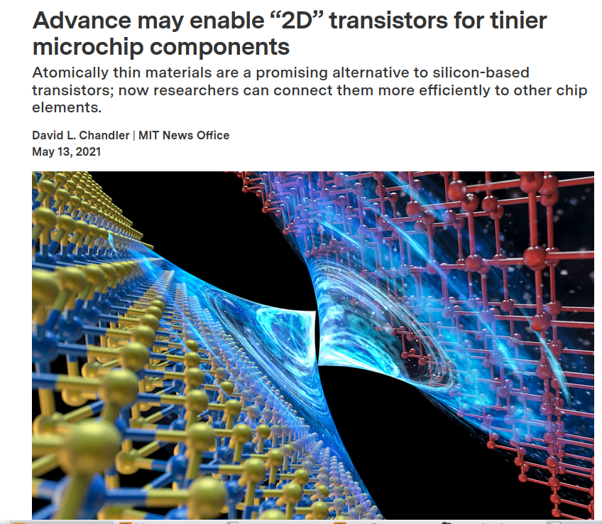
https://news.mit.edu/2021/2d-transistors-microchip-0513
https://www.youtube.com/watch?v=sJwT0j1VGps
May 15, 2021 9:54 AM
TamilTechNews
99494
1781
17
https://news.mit.edu/2021/2d-transistors-microchip-0513
https://www.youtube.com/watch?v=sJwT0j1VGps
netutoring
Science, you are one crazy mother... and I love it.
MisterLemons
I guess that's as small as we can make common computers then? We're not aligning quarks before quantum computing...
ThicclikePaulBunyan
Good news......BUT THAT DOESN'T HELP BUYING A NEW GPU!
b1candy2
End users who buy 1 at a time aren't the priority.
GiuseppeW
It's interesting watching technology coming to the the of it's physical limits. Pretty soon it's quantum or stagnation
theimgurappsucksballs
MelfsAcidArrow
What I love about this is that some production assistant had to write all those 4’s for real
EnochNek
This new technology will require an extra layer between every metal contact factoring in that designs already have multi level contact point
EnochNek
This will not play out as simple as advertised. The net benefit may not actually be smaller
FreeRangeToast
I have the technological understanding of a concussed aardvark, so I missed a lot of this, but still very neat. +1
apostlepk
3/5 the way finished with my masters in electrical engineering, and I still feel like I'll never understand this kind of shit. Wow.
captainclutch
What we need is software that's better at handling multiple cores. I can encode a project from Premiere or AE and use 100% of a single core
captainclutch
while the other 7 just sit there and watch
Someshithead241
NANOMACHINES SON!
JackTheRippersBrotherHowie
cuz the current ones are getting stuck in the covid needles?
hairbearbunch66
I hope the nanobots that destroy life make something pretty
opi098514
“The solution proved to be a simple one” Just make it smaller lol
mouseasw
All I'm seeing is Moore's Law continues to hold true because we find new solutions when the old solutions reach their physical limits
EnochNek
The obsession with followings moores law is stupid and is holding humanity back from developing actual advances in technology
MightyIink
For those wondering of the applications, it would mean we would finally break the 5 GHz barrier on consumer CPU's.
RVME
That's what transistors were when I made them. JFET's are 3D junctions. This needs more 'splaining.
DaveSamsonite
There are still bias in the z axis. Have to be.
DaveSamsonite
VIAS, not bias
giganticroboticpenguin
I have been wondering why they didn't make 3D circuits 20 years ago (I knew someone who worked at Intel then but not in design).
dreikommavierzehn
If I remember correctly it was about costs. Intel was very successful by improving their existing methods and published several news over >
dreikommavierzehn
the years where they debated the pros and cons of staying course vs. shifting their resources towards a different approach
dreikommavierzehn
I remember reading that the stacking approach was delayed until the micronization wasn't worth the effort anymore
Elroydb
There's a limit to this. Imagine having your computer crash due to the Heisenberg Uncertainty Principle
EnochNek
Thats a quantum computer friend
Elroydb
That's where we have to go. The current architecture where components are built so close together will have this problem
IlluminaBlade
I swear I saw people say that transistors are getting so small that cosmic radiation is causing computer errors.
TheyDontKnowAndYouCantTellEm
Transistors on IC's are already 2D. Utterly stupid headline.
TheyDontKnowAndYouCantTellEm
Go ahead, downvote an IC designer.
Rifneno
Imgur hates actual science. That's why This Week In Clickbait always gets so much love.
thedudeman519
Well, since you asked nicely .
erroniousmaximus
Maybe. Just maybe. It’s the lack of additionally information that makes you come off as a penchant dickhead, rather than an expert?
TheyDontKnowAndYouCantTellEm
Maybe the people who write headlines who don't have a fucking clue about technology are the REAL dickheads. Amateur writers.
TheBestSpiderQueen
Maybe just maybe headlines aren't meant for communicating high level ideas.
[deleted]
[deleted]
TheHuntedSnark
"The solution proved to be a simple one" - that's obviously when the article becomes more complex.
EnochNek
They use a different material that requires an inbetween material to make up for the metal gap. Its not complicated but it wont work well
CrypticalEnvelopement
Semiconductors are made out of nonmetals, and are generally poor conductors of electricity. What's cool about semiconductors is this can 1/
CrypticalEnvelopement
Be changed to make them highly conductive, and this is the opening and closing of logic gates that makes computers work. The researchers 2/
CrypticalEnvelopement
Reduced these gates down to the width of a single atom, but at such small scales the difference in electrical properties between the 3/
CrypticalEnvelopement
Metal of the circuits and the nonmetal of the gate wouldn't allow electricity to flow. The solution was to glue them together with a 4/
CrypticalEnvelopement
Semimetal, effectively blending their properties. It's like washing oil with water, you use soap to bind the oil and water together.
bsmithwins
It’s never been simple since the invention of mechanical computers
MCNewYorkLives
I mean, just make it smaller. How difficult could it be? /S
nasukkin
Well... We're pretty much at the physical limit of how small they can be. So, the next big challenge is to figure out the best ways to...
nasukkin
... pack more of them into a small place. This seems to be one of those innovations.
DVSBSTrD
It usually is simple, just hard as fuck to get there.
Rogahar
I feel like a lot of specialists look back at whatever the last big leap was and think "how the fuck did we ever miss that before?"
DVSBSTrD
Oh hell yeah.
Rogahar
It astounds me to think that one day we'll look back on whatever unlocks teleportation or FTL travel or viable large-scale terraforming like
Rogahar
that too. Like 'Jesus christ we were so stupid the solution was right infront of us for like 500 years.'
FoxyEllie
The problem is there's billions of possible simple ways for things to work, you gotta find the right one
ElSephiroth
Not really because some are real hard to confirm. Take cern for exemple. Massive and massively complex. But sometimes, yes:carbon pen+scotch
DocHarriers
I saw something on reddit the other day about 2nm technology. A linked video said that the connections being so thin is a problem, as well
b1candy2
Link to the reddit thread?
DocHarriers
as leakage inside the transistor. I am looking forward to reading this to find out how they get around the limitations.
LespritDeLescalier22
Heehee *leakage*
BunnyBooBear69
What gets me is that that's not even 10 atoms thicc. (Si = 210pm = 0.210nm)
b1candy2
2nm is a marketing name as if it were planar, but as it's a 3D Transistor it's obviously a lot bigger
UWAGAGABLAGABLAGABA
If they would stop using silicon, and transition to synthetic diamond, leakage wouldn't be a thing.
jcod
I'm interested if it is viable for synchronous circuits. Clock distribution will be hell when we keep shrinking signal/noise.
ufretin
2nm isn't actually 2nm transistor size. They still haven't gone below 22nm-ish transistor size. They have purely uptimized the x/2
ufretin
connections between the transistors. So they become much more power efficient.
ufretin
The proces they use is uses extreme ultra violet light to make a transistor pattern. Extreme ultra violet light can only be made with a
ufretin
sapphire, which they superheat, so that it generates plasma, that emits sub 185nm lightwaves. Which they etch into the silica disc over
jansenart
Spoiler: they don't. They're doing stuff a QM PhD could tell them was a waste of time but they do it just to be funded.
Zefster
the 2nm stuff is mostly marketing afak they're layering bigger transisters and saying theyre smaller
DocHarriers
Yep. Shape of the gate to make for less off-state leakage was interesting, too.
ImJustHereBecauseILikeMemes
^ this. The act of layering allows for the lower power consumption and increased performance as if it was a traditional chip at 2nm.
accidentalholocaust
It's a different way of measuring it, so not entirely marketing